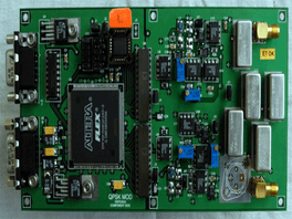
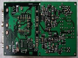
PCB Layout design From Schematic & Fabrication
- Ambimat’s layout design was a mix of digital and RF components on single six layers PCB. The digital section comprised of an FPGA along with associated buffers, drivers etc. The RF section consisted of two-way 90-degree power combiner/splitter, SPDT Switch and Power Amplifier for RF signal for transmission.
- The modulator was successfully subjected to 168 hour burn-in environmental testing.


